 issie
issie
Getting Started
Downloading and Running ISSIE
Find the latest ISSIE release. At the bottom of the page, you can find the latest pre-built binary for your platform (Windows or ARM64 Macos). ISSIE will require in total about 200M of disk space.
- Windows: unzip *.zip anywhere and double-click the top-level
Issie.exeapplication in the unzipped files. -
MacOS: Double click the dmg file and run the application inside the folder, or drag and drop this to install.
- The MacOs binaries are signed.
-
If you can't find a binary:
-
MacOs binaries are sometimes not uptodate. You can always generate your only binary by
setting up for development and running
npm run dist. This will not need to be signed if runnng on your own machine. Note that you do not need to edit source code to generate a binary. - You can look through previous releases to find the last posted binary for your system. However ISSIE newer releases often have significant new functionality and bug fixes. It is best to have the latest release,
-
MacOs binaries are sometimes not uptodate. You can always generate your only binary by
setting up for development and running
Creating a New Project
Once you open ISSIE you should see two options: New Project and Open Project.
- Click
New Project - Navigate to the folder you want to save your project
- Enter the name of your project
- Click
Create Project
This process creates a folder where your project will be stored and the first sheet of your project, called main. You can see this by clicking at the Sheets selection button.
Your first design
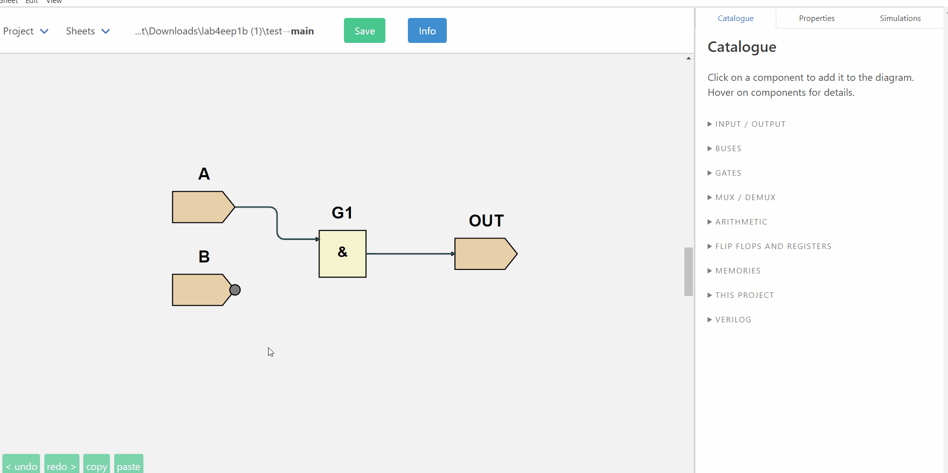
Let's start with a very simple schematic: a simple 2-input AND gate.
Add the following components to your canvas from the Catalogue tab:
INPUT/OUTPUT=>Input=> Name: 'A', Bits: 1INPUT/OUTPUT=>Input=> Name: 'B', Bits: 1GATES=>AndINPUT/OUTPUT=>Output=> Name: 'OUT', Bits: 1
Now make the appropriate wiring to connect all the components by clicking on one port and dragging the wire to the port you want to connect it to.
Connect:
- Input 'A' to the first input port of the AND gate
- Input 'B' to the second input port of the AND gate
- Output 'OUT' to the output port of the AND gate
Your design should look like this:
Simulation
Time to simulate the design and see how the output OUT changes as we change the two inputs.
Click the Simulation tab which is located on the top-right corner and then Start Simulation. Now you can change the value of the two inputs and see how the value of the output. Try all 4 combinations of inputs:
- A=0, B=0
- A=0, B=1
- A=1, B=0
- A=1, B=1
and check that the output is correct based on the truth table of the AND gate.

Well Done! You just completed your first ISSIE design.
Exploiting the ISSIE Features
A slightly more complex design
This section will exploit the features of ISSIE to create clean and good-looking schematics when making bigger designs.
- Add two more inputs named
CandDeach 1-bit. - Add one OR gate and one 2-input MUX
-
Delete the output
OUT- Note: You can delete components and/or wires by selecting them and clicking the
deletebutton on your keyboard
- Note: You can delete components and/or wires by selecting them and clicking the
- Add a new 1-bit output
RESULT - Make all necessary connections by dragging as before to achieve a diagram like the one bellow:
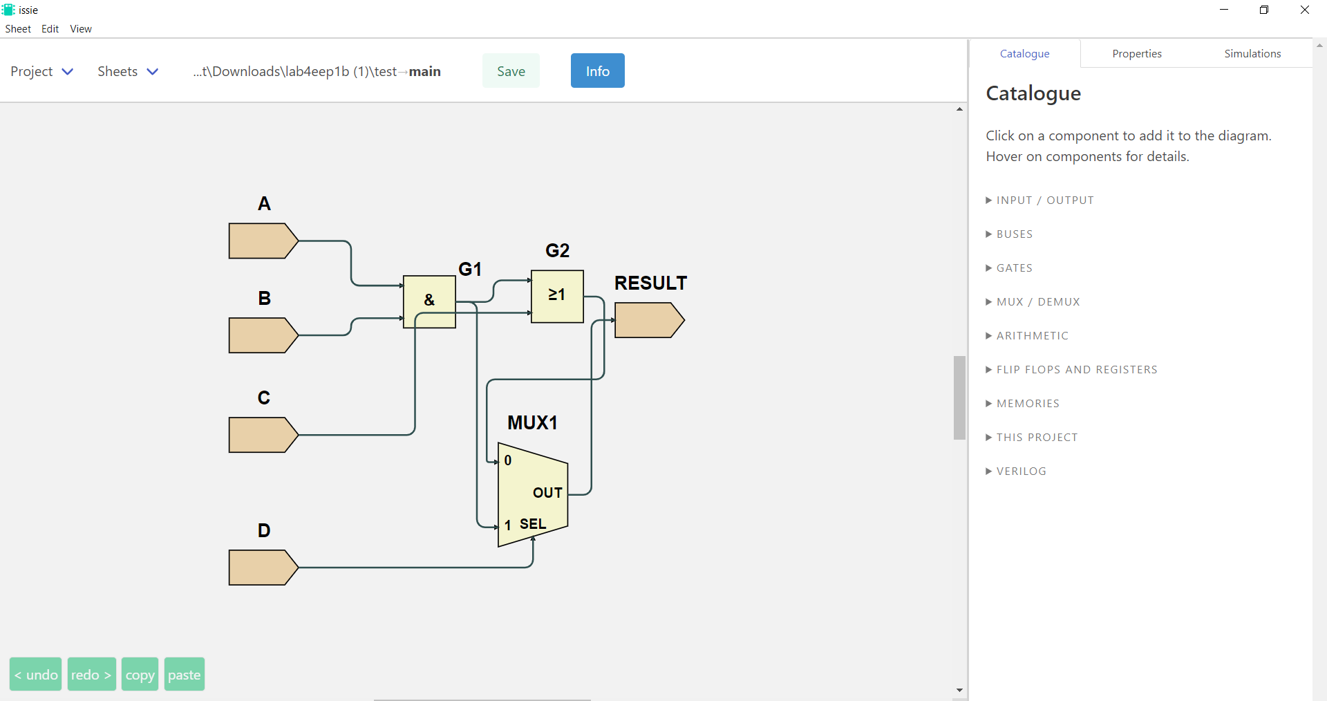
Again, simulate the design and check the output remains correct as you change the values of the 4 inputs
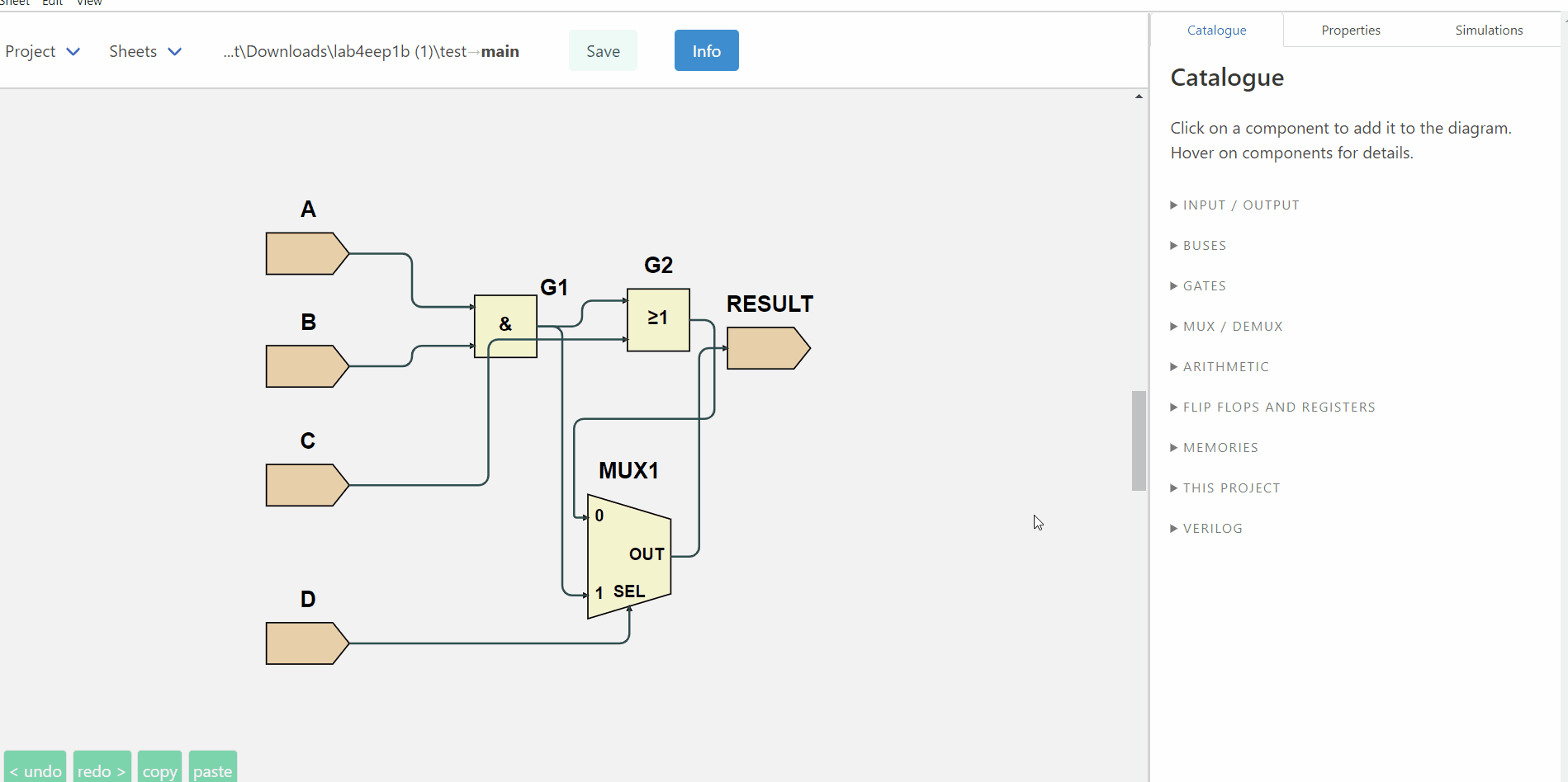
Improving the look of a schematic
The schematic here is not easy to read. Let's improve it! The ISSIE canvas is fully customisable to allow the creation of readable and good-looking schematics. Specifically, we can:
- Rotate, Flip and Move all symbols
- Change name and reposition the symbols' labels relative to the symbols
- Manually route any specific segment in a wire
- Auto-align elements
- Select the desired wire type (radiussed, jump or modern wires)
You can view the shortcuts for all these modifications by clicking on the edit and view menus.
The improved schematic:
Summary
- In the
CatalogueMenu we can find an extensive and complete library of components (gates, flip-flops, RAMs, ROMs, n-bit registers) - We can add any number of components in our sheet and name them as we like
- When clicking on a port, ISSIE shows us all the ports we can connect that port to: dragging from one port to another makes a wire.
- Wires are initially automatically routed
- Auto-routing can be selectively over-ridden by manual routing to make a better-looking schematic.
- We can simulate our design and check how the outputs change as we change the inputs.
Using Custom Components
The root schematic
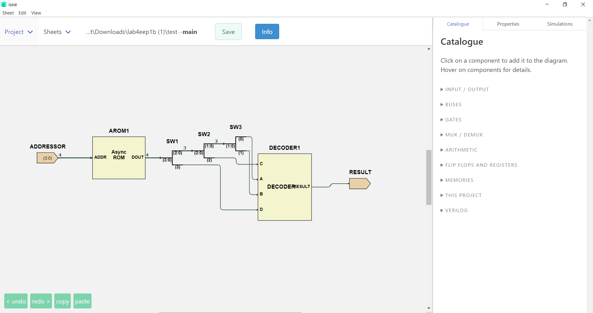
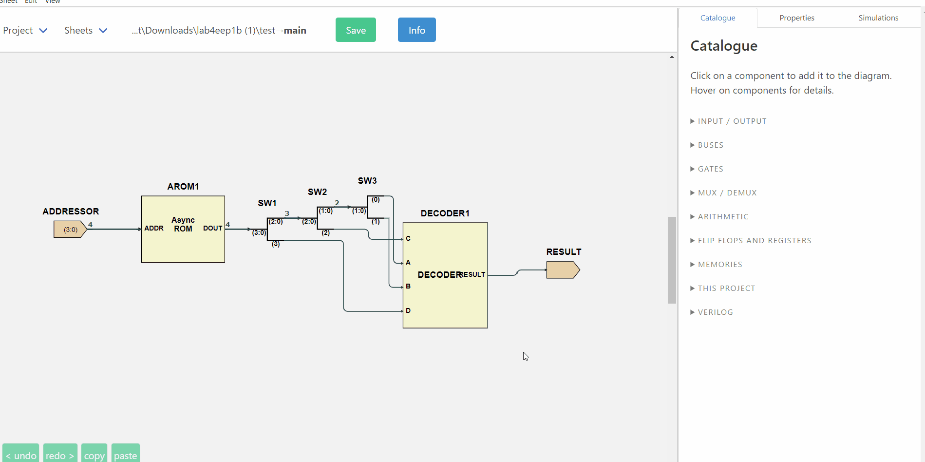
In this section we will create a hierarchical design with multiple design sheets by using schematics as custom symbols in other design sheets. Here is the aim: The design we created earlier can be used in a larger design as a decoder of a 4-bit message to produce a true/false result. Therefore, we are going to create a schematic with an asynchronous-read 4-bit ROM using the schematic we created before as a custom symbol.
Steps
- Change the name of the current sheet from
maintodecoder(Sheets -> rename) - Add a new sheet and name it
main -
Add to the main sheet:
- Asynchronous ROM (
MEMORIES=>ROM (asynchronous)). Select 4 bits addressor, 4 bits data and theEnter data lateroption - Your decoder (
THIS PROJECT=>decoder) - 1-bit output named 'RESULT' (
INPUT/OUTPUT=>Output) - 4-bit input named 'Addressor' (
INPUT/OUTPUT=>Input)
- Asynchronous ROM (
- Using 3
SplitWirecomponents (BUSES=>SplitWire) separate the 4-bit ROM output to 4 1-bit wires. (see image below) - Make the appropriate connections to achieve the schematic below
Improving the design sheet
It's time to use a hidden part of the ISSIE UI to move ports on custom symbols. ISSIE allows you to re-order and change the side of input and output ports of custom symbols by CTRL + CLICKING ON THE PORT you want to move. The UI, once you realise that you must keep Ctrl (Cmd on Macs) pressed, is intuitive.
Preview how it works in the gif below:
ROM Initialisation
Currently our ROM is empty as we selected the option Enter Data Later before. Let's put some values in our ROM.
- Select the ROM and click on the
Propertiestab - Click on
view/edit memory content - Change the content of the 16 memory location available by assigning a random 4-bit number to each one
- Click
done
ISSIE also allows ROM and RAM initialisation via .ram text files of hex data in the ISSIE directory. See the ISSIE Eratosthenes demo for an example of this. The memory component properties tab offers additional options when there .ram files present.
Simulation
Simulate your design! Change the value of the addressor input and see whether your decoder produces a true or false result for each number you assigned to the ROM.
Waveform Simulation
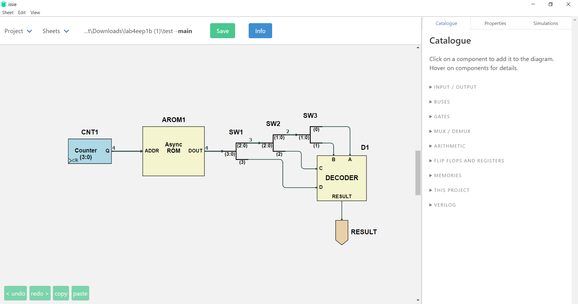
Creating a clocked design
Let's now modify our previous design to make it clocked (sequential). We use a counter to form a custom addressor that will increment every clock cycle. Using the waveform simulator we will be able to view the output of our circuit for all memory locations. In order to create such designs easily, ISSIE offers a Counter component which, starting from 0, increments by one every clock cycle. Note that counters also have options, under properties, to add Load or Enable inputs.
Add a Counter from the Catalogue (FLIP FLOPS AND REGISTERS). Now select the component and click on Properties. In properties remove the load and enable ports and give them the default functionality (which is what we want in this case): enable=1; load=0;
Edit the previous design to create a schematic like the one below:
Simulating your design
As soon as you connect everything correctly, You can simulate your design. Click on Simulations and then Wave Simulation.
- Click the
Start Simulationbutton - Click
Select Waves
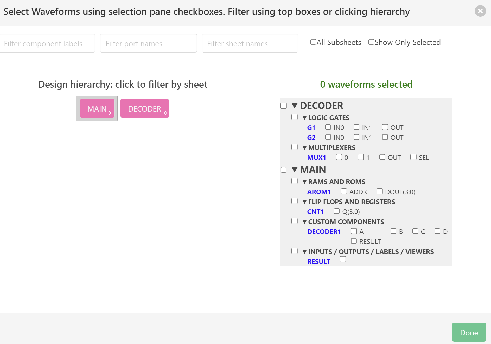
- Click the
Mainbreadcrumb to filter so only main sheet ports are visible.
-
Select:
AROM1 AddrCNT1 Q[3:0]DECODER1 RESULT
- Click
Done -
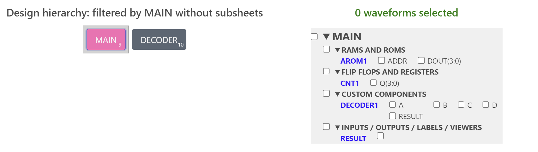
To check what you have selected:
- Click
Select waves again - Click
Show only selected - Click
Done
- Click
- Use
Select RAMto select the ROM contents to view. - Change the data format to either
hexorbinto make the waveforms more readable - adjust the number of clock cycles displayed using the
+/-zoom controls. - Order the waveforms
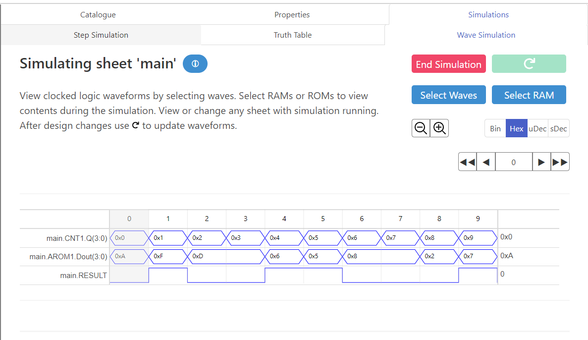
CNT1 / AROM1 / RESULTby dragging the waveform names up or down. - Check that the waveform simulator output matches your previous (Step Simulation) results.
- Use the scroll bar to view additional clock cycles.
- Drag the grey horizontal divider to make the waveform display wider or narrower (you can do this at any time).
- You can check how these features work on a much larger design with 100,000 clock cycles using the Eratosthenes sieve demo.
Changing your design
Now, keeping the simulation open, add an extra register between the counter and the ROM address (or make any other change you want) and check that the simulation has the expected output. You can see the changes in the waveform simulator by clicking the Refresh button which will be enabled as soon as there is a change in the schematic.

Truth Table
One of ISSIE's features is the ability to view the truth table for a small combinational circuit.
- Click on
Simulationsand thenTruth Table - Select the
DECODERcomponent - Click on
Generate Truth Tablebutton on the 'Truth Table for selected logic' section - Click on
Remove Redundancies - The truth table should look like this:

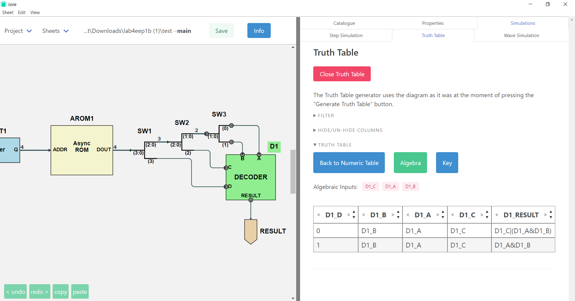
You can also select your inputs to be algebraic values to get an expression for each of your outputs.
- Click on
Back to full table - Click on
Algebra - Select the inputs (
C,B,A) you want to be algebraic values - Truth table should now look like this:
Verilog Component
Last but not least, ISSIE allows you to create combinational custom components by defining the logic in Verilog. Click on Verilog -> New Verilog Component (Catalogue) and write the logic of your decoder in Verilog.
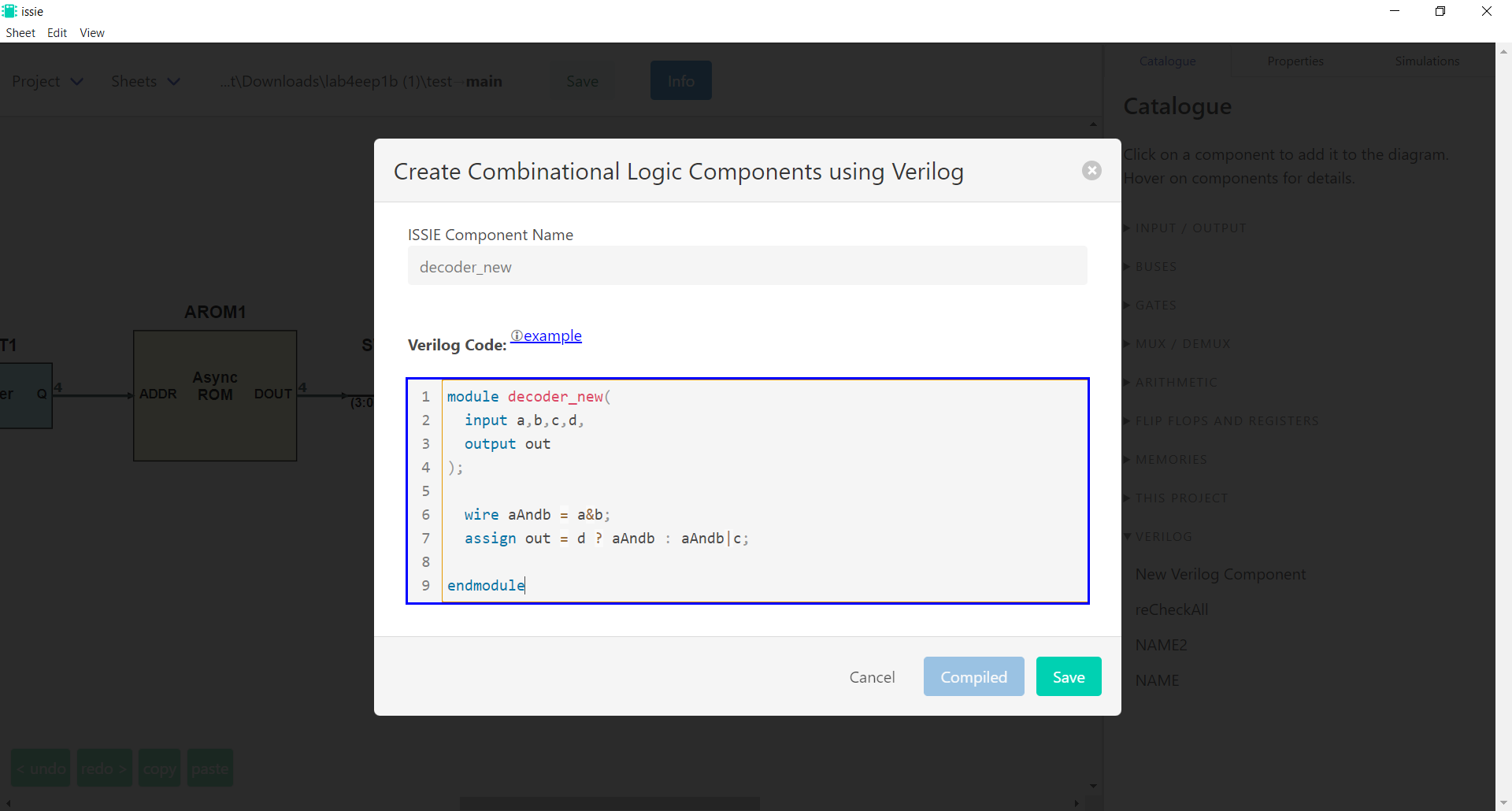
- Click
Save - Replace the previous Decoder with the new one (found under
Verilogsection in the Catalogue) - Simulate again your design. Everything should be the same as before.
Now what?
You now know how to use ISSIE to create & simulate digital designs.
You can now create your designs (from simple circuits to fully functioning CPUs) and either simulate them or extract them as Verilog to use them with other tools.
For inspiration, look when you start ISSIE under the demos option for Eratosthenes Sieve demo which consists of an EEP1 CPU running an Eratosthenes Sieve program written in EEP1 assembly language. The sieve occupies most of EEP1 RAM and the program takes 200,000 clock cycles to run.